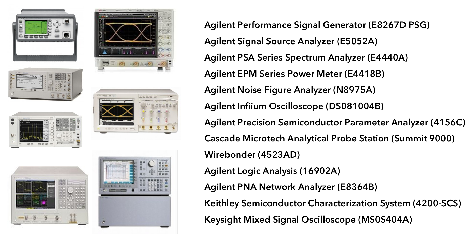
Test & Measurement
CEDEC has a suite of equipment for RF, digital and mixed-signal applications to cater various measurement needs. CEDEC can support on-wafer measurement (up to 8 inch wafer), on-chip measurement (die probing), on-board measurement and even outdoor measurement. With all of these equipment, CEDEC provides test and measurement services for research and development purposes.
To let us understand your test requirement, we would like you to provide the following information while contacting us:
- Type of test (On-Wafer, On-Packaged, On-Board or even outdoor test
- Type of application (RF, Digital or Mixed-signal)
- Name of the board or device
- Parameters or equipment needed
- For On-Wafer testing, layout of the device with pad assignment must be provided (The pad configuration must be designed according to CEDEC's Avilable probe)
- Other constraints need to be considered
For more information regarding the Test and Measurement at CEDEC, please do not hesitate to contact or consult with our staff:
Mrs Sofiyah Binti Sal Hamid
Collaborative Micro-electronic Design Excellence Centre (CEDEC)
Sains@USM, Level 1, Block C
No 10, Persiaran Bukit Jambul
11900 Bayan Lepas
Penang, MALAYSIA Phone: +604-653 5622
email: sofiyah@usm.my