Multi Project Wafer
The CEDEC Multi-Project-Wafer (MPW) coordination with Silterra program is intentionally introduced whereby the participants from the local institutions will benefit an affordable fabrication cost for the design utilizing 0.18um, 0.13um or 0.11um Silterra CMOS technology (for Malaysian university ONLY). Multiple projects will be placed in a single wafer where the whole mask cost is shared together.
MPW new structure begin in late 2010 in which shows the close cooperation between CEDEC and Silterra. Initially Silterra is responsible for receiving each GDSII file that is sent by the universities in Malaysia for the fabrication, but in forming the new structure, CEDEC works with Silterra to expedite the process for the chip designed by the university.
CEDEC has partnered with Silterra in Malaysia to allow the later process technologies be made available for low-cost prototyping to universities through a multi-project-wafer (MPW). At present the following MPW technologies are available from Silterra.
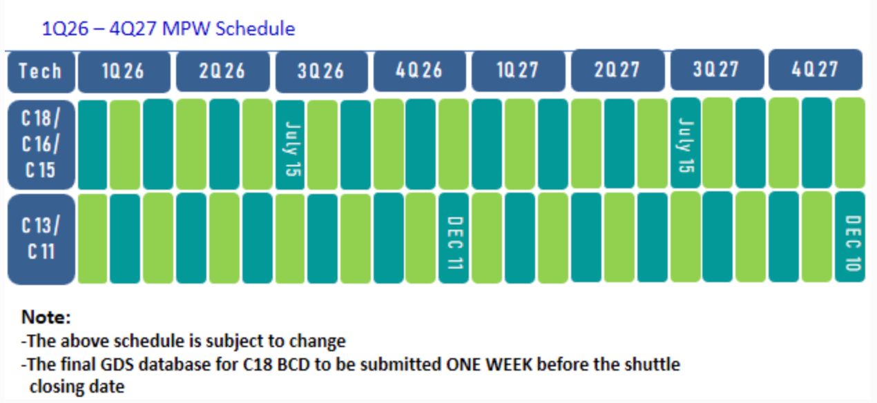
2026-2027 MPW Schedule

Note:
- The above schedule is subject to change.
- The final GDSii file, DRC summary report file, LVS report file and DIFFCAD form to be submitted during CEDEC's shuttle due date.
- GDS2 file to be received by mpw@usm.my two (2) weeks before tape-out date.
- The above schedule is subject to change.
- The final GDSii file, DRC summary report file, LVS report file and DIFFCAD form to be submitted during CEDEC's shuttle due date.
- GDS2 file to be received by mpw@usm.my two (2) weeks before tape-out date.
CEDEC will permit customer to participate in Multi-Project Wafer (silicon Verification) programme where fabrication of chip designed by customer will be carried out at Silterra Malaysia Sdn Bhd on a special rate basis.
(*) Each for 20 bare dices with 2mm x 2mm
Please send to us the following documents:
- Application form [download here]
- GDSII file
- DRC and LVS report files
By Purchase Order (PO) from university treasurer party / bursarydepartment of your university
1. Release PO under the name of Bendahari USM after CEDEC sent a quotation.
2. Send original copy of the PO to:
Collaborative Micro-electronic Design Excellence Centre (CEDEC)
Sains@USM, Level 1, Block C, No. 10,
Persiaran Bukit Jambul,
11900 Bayan Lepas,
Pulau Pinang.
Attention: MPW Administration
3. Please proceed for payment after received the invoice from CEDEC.
For further assistance, please email to :

